There are two technologies currently trending in the practice of stencil making for screen printing.
First is the increasingly popular use of Photopolymer emulsions to replace 2-part products. There are many reasons for this switch over, with the main benefits being the faster exposure speed & longer shelf life of Photopolymer products. The second trend is a rapid conversion towards using LED’s to perform screen exposure. Anyone who has attended a screen printing exhibition recently can attest to the rapid proliferation of LED exposure systems on display.
The purpose of this article is to outline the working relationship between PVA-SBQ polymer, the raw material used for manufacturing Photopolymer stencil materials, together with the type of LED light that is required to expose these stencils (curing & imaging), in order to guarantee optimum results.
PVA-SBQ polymer, aka Photopolymer is a modified form of Polyvinyl alcohol, aka PVA. PVA polymer is an essential component of all direct stencil materials, because of a unique combination of three properties. First, it is water soluble, so that emulsions are water based and stencil developing can also be performed with water. Second, PVA is very solvent resistant, unlike most other water soluble polymers that are even more soluble in solvents than in water. Third, it contains a glitch in the polymer chain, as a normal result of the manufacturing process. This allows stencils to be broken down and screens easily reclaimed, under mild conditions, using water based reclaiming solutions. PVA is used universally in all direct emulsions and capillary films, and many different grades are available. This allows manufacturers a high degree of flexibility to modify technical properties for a wide range of emulsions.
To convert PVA to PVA-SBQ, the PVA polymer is modified by attaching cross-linkable SBQ molecules to the polymer chains. Each attached molecule contains a chromophore. This is a dye like structure, that renders the PVA-SBQ polymer light sensitive. This group also performs double-duty, by being able to react and crosslink the polymer during exposure. The level of SBQ addition onto the PVA is quite low, normally only 1-2% substitution of the PVA groups. In this case, the final PVA-SBQ polymer retains all of the desirable properties of the original PVA, including water solubility, solvent resistance & ease of reclaiming.
See Figure 1 for an illustration of PVA-SBQ polymer with the essential parts highlighted.
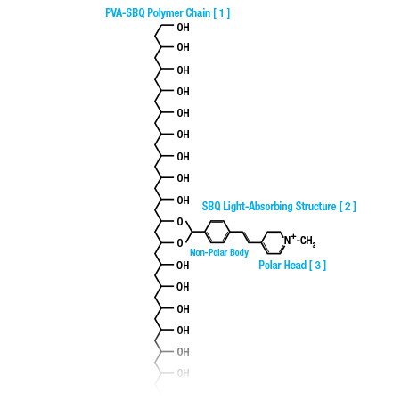
Figure 1
1). PVA-SBQ polymer chain – retains original technical & chemical properties of PVA
2). SBQ photo-sensitizer – light sensitive crosslinking group
3). Hydrophobic (non-polar) body joined to hydrophilic (polar) head – similar structure & properties as a surfactant.
The PVA-SBQ polymer is very light sensitive, even at low levels of SBQ content, because of the surfactant like structure of the light sensitive groups that enables them to associate with one another. After coating & during drying, when the liquid emulsion produces a dried film on the mesh, isolated SBQ groups are able to seek & find each other. The alignment that results is shown in Figure 2.

Figure 2
This fortuitous arrangement enables two adjacent groups to be perfectly placed, then react quickly on exposure to crosslink the polymer, as shown in Figure 3.

Figure 3
This ideal alignment scenario occurs only for a proportion of the attached cross linking groups, but it’s enough to allow the preparation of fast exposing stencils that have good cross link density. By varying the formulation of emulsions, manufacturers have the ability to produce a wide range of products. These Photopolymer emulsions enable stencils to be prepared & printed, and used as robust replacements for older two part Diazo & Dual-Cure products in all industry segments, including textile as well as industrial & display graphics.
The light absorbing properties of the PVA-SBQ play a major role in determining thorough curing of stencils. Typical screen printing stencils range from several tens of microns total thickness, up to several hundred microns, depending on the mesh count used and the coating sequence. Total thickness includes the EOM, or stencil profile, plus the emulsion that’s embedded and encapsulates the mesh, to provide both adhesion during developing, and durability during printing. The stencil exposure process is about more than just simply defining the image to be printed. It must also be optimized to ensure thorough curing of the full stencil thickness. Full cure is required to maximize durability and printing life, and this aspect becomes even more critical when using very aggressive inks, such as textile printing with water-based, or discharge ink.
Use of LED’s for screen exposure offers many advantages, including low power consumption, cool running, extended lamp life & mercury free construction. Also the ability to use a simple timer to control exposure, instead of photocells & light integrators, because LED light output is stable and constant unlike metal halide bulbs that gradually degrade and lose intensity. LED exposure is also now widely used in computer to screen imaging, including direct to screen image-setter systems, such as the CST DLE, as well as in-line exposure inkjet masking systems, such as M&R I-Image STE range of products.
Because LED’s are designed to emit a very narrow band of very high intensity light, the selection of LED wavelength now becomes critical. There must be a good match between LED output and PVA-SBQ sensitivity in order to ensure best chance of thorough stencil curing and wide exposure latitude. A poor match will yield inconsistent results, maybe with success on thinner coatings, but failure when stencil thickness is increased, or lower mesh counts are used.
Figure 4 shows the absorbance spectrum of a very thin film of PVA-SBQ polymer.
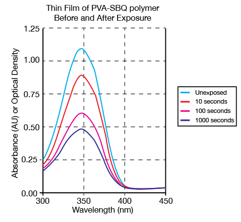
Figure 4
The SBQ chromophore is a powerful light absorber, and maximum absorbance occurs in the UV part of the spectrum, that’s below 400nm. Also shown is the result of exposing this film and the ‘bleaching’, or reduction in absorbance that occurs during exposure. Bleaching happens when cross-linking consumes the reactive groups. This lower absorbance is shown after 10s, 100s, or 1,000s exposure time. It’s clear that longer exposure times reduce the absorbance, but there’s a problem. Typical exposure times required to make high quality stencils, with good resolution, consume only a fraction of the available reactive groups. These happen to be the ones that were perfectly aligned during drying of the coating, and are well placed to react quickly. Extended exposure times can cause additional reaction, but are not practical because of degradation in stencil quality due to loss of resolution. In any case, it’s clear that even extremely long exposure times, up to 100X over-exposure, cannot reduce the residual UV absorbance of the coating down to zero.
This has serious implications for use of UV light emitting LED’s, for example 365nm or 385nm LED’s. Light of these wavelengths is so strongly absorbed that it cannot penetrate the full thickness of the coating. Matching the LED output wavelength to the absorbance spectrum of the coating might seem like a sound idea, but in practice yields poor results.
Figure 5 and 6 show respectively the absorbance & transmission spectra for a typical coating of PVA-SBQ polymer, one that would be thick enough to be used as a stencil for screen printing.
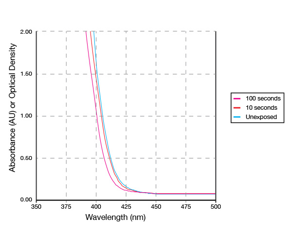
Figure 5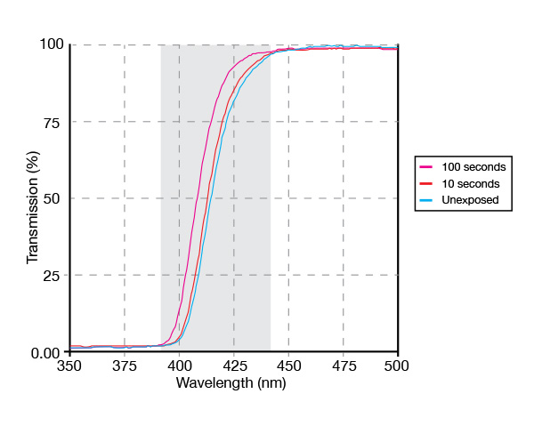
Figure 5
This thicker film now displays very high optical density, and absorbance goes basically off the scale at UV wavelengths, even after extended exposure times. As Figure 5 shows, absorbance is >2 at UV wavelengths below 390nm.
For reference, absorbance and optical density can be used interchangeably, and a density of 1 AU (absorbance unit) is equivalent to blocking 90% of the light, or equivalent to 10% transmission. Density of 2 AU blocks 99% and allows only 1% transmission, and so on. Typically a density of 3+ is desired for high quality film positives.
Consequently, the very high absorbance, and almost zero % of light transmission below 390nm for a typical coating means the coating is essentially opaque to UV light. Since UV light is unable to penetrate the full thickness of the coating, it therefore cannot be responsible for exposing deeper layers of the stencil.
More important, it’s also now apparent that the tail of absorbance curve actually extends beyond 400nm and into the blue part of the actinic light spectrum. Although the absorbance around 400nm looks weak, or even nonexistent, when looking at the spectrum of the thin film in Figure 4, it’s clear that thicker coatings, as shown in Figure 5, do in fact display strong absorbance. Our typical coating used for stencil making in this case absorbs more than 90% of the available light at 405nm, and the stencil is very sensitive to exposure at 405nm. So, it’s now very apparent that maximum Absorbance and maximum Sensitivity are not the same thing.
The light transmission spectrum illustrated in Figure 6 also shows that the PVA-SBQ coating becomes 100% transparent to light above 440nm, and light that is not captured cannot be used for crosslinking. In practice, there is a narrow band of wavelengths, above 390nm & complete opacity, and below 440nm & complete transparency, where light is absorbed strongly enough to crosslink a stencil, and yet is still able to penetrate and expose the full thickness of the coating to ensure durable stencils.
This effect is illustrated in Figure 7 and shows the relative ability of light from commonly used LED’s to penetrate and cure a coating, to expose and create a stencil.
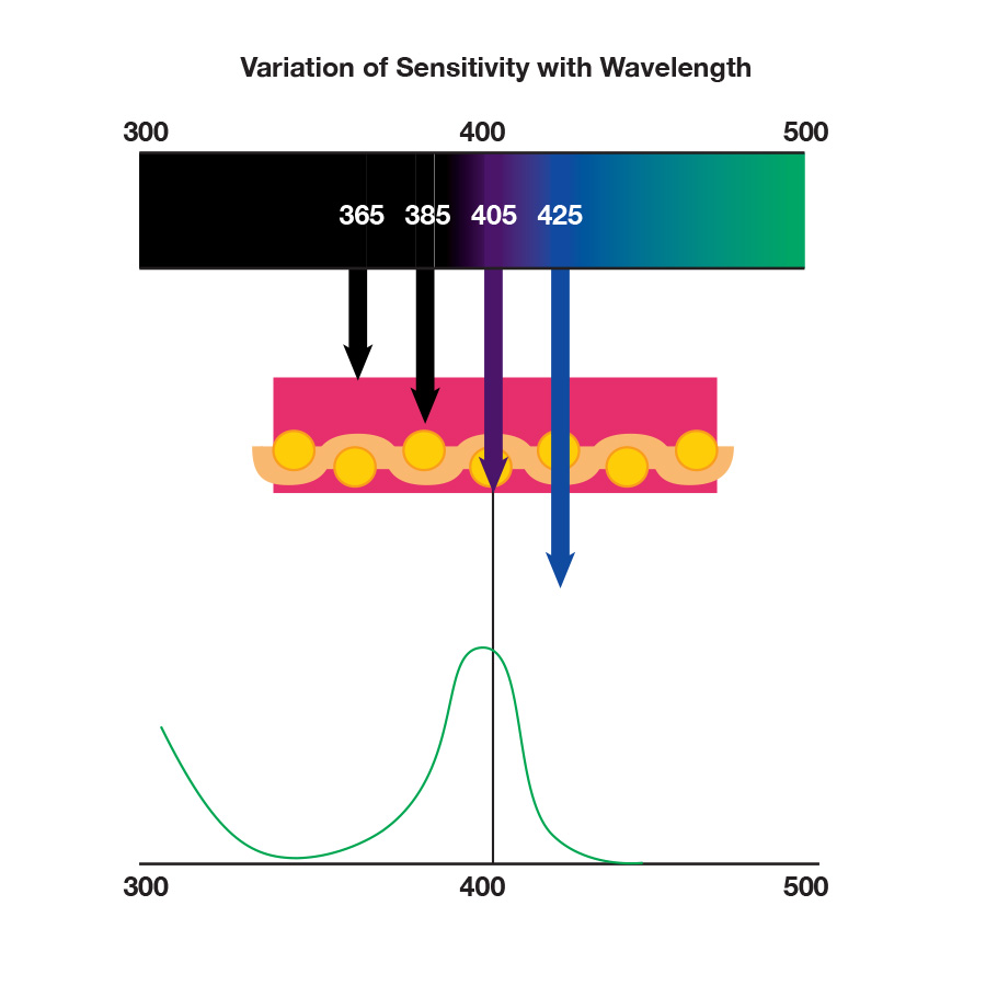
Figure 7
The depth of light penetration into the coating = cure depth. Cure depth is heavily dependent on wavelength. Stencil adhesion & durability are directly related to cure depth.
- 365nm low sensitivity – only surface cure because stencil too opaque
- 385nm cannot penetrate thicker coatings – poor exposure latitude
- 405nm penetrates deeply – optimum stencil cure & exposure latitude
- 425nm is too weakly absorbed – poor cure because stencil too transparent
So, there is a practical relationship between Wavelength and maximum Sensitivity, which peaks around 400nm, and is driven by depth of cure requirements for the relatively thick layers that must be exposed to produce a typical screen printing stencil.
Another way to illustrate the relative efficiency of commonly available LED’s is shown in Figure 8. This also shows the relationship between absorbance and sensitivity, and they are clearly NOT the same thing.
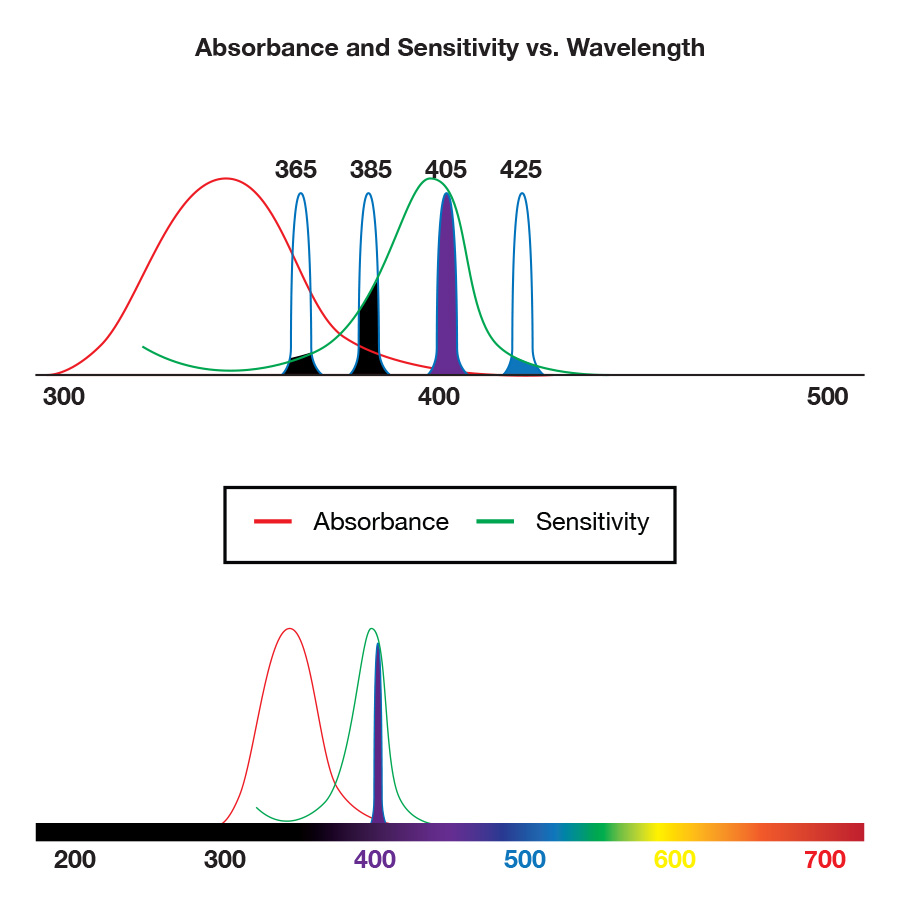
Figure 8
The ideal overlap of 405nm LED actinic light output, with the sensitivity curve of PVA-SBQ polymer, makes this type of LED the best replacement for traditional metal halide bulbs that previously represented the gold standard for exposure lamps.
In fact, now that we have established a sensitivity profile, a similar analysis can be carried out that compares light output of traditional mercury vapor UV lamps and metal halide lamps. Metal halide lamps are basically just mercury vapor lamps that are doped with additives. The additives are used to provide enhanced light output at actinic violet & blue wavelengths. These doped metal halide lamps are very widely used, and it’s commonly accepted fact they far outperform the basic mercury vapor version, that is little/never used to make screen printing stencils. This comparison is illustrated in Figure 9 and shows the overlap of the sensitivity curve with the relative intensity of light output from both these lamps.
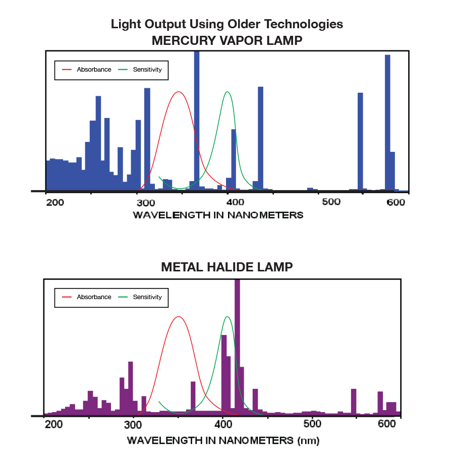
Figure 9
The excellent overlap of sensitivity curve with the light output of metal halide lamp provides further confirmation that it is enhanced violet/blue actinic light output, and not UV, that is most effective in curing screen printing stencil materials. It also further confirms 405nm LED as the most suitable choice for metal halide replacement.